
Author Affiliations
Abstract
1 Centre for Optical and Electromagnetic Research, State Key Laboratory for Modern Optical Instrumentation, Zhejiang Provincial Key Laboratory for Sensing Technologies, Zhejiang University, Zijingang Campus, Hangzhou 310058, China
2 Ningbo Research Institute, Zhejiang University, Ningbo 315100, China
3 imec USA, Nanoelectronics Design Center, Inc., Kissimmee, Florida 34744, USA
4 Ocean College, Zhejiang University, Zhoushan 316021, China
All-optical silicon-photonics-based LiDAR systems allow for desirable features in scanning resolution and speed, as well as leverage other advantages such as size, weight, and cost. Implementing optical circulators in silicon photonics enables bidirectional use of the light path for both transmitters and receivers, which simplifies the system configuration and thereby promises low system cost. In this work, to the best of our knowledge, we present the first experimental verification of all-passive silicon photonics conditional circulators for monostatic LiDAR systems using a nonlinear switch. The proposed silicon nonlinear interferometer is realized by controlling signal power distribution with power-splitting circuits, allowing the LiDAR transmitter and receiver to share the same optical path. Unlike the traditional concept requiring a permanent magnet, the present device is implemented by using common silicon photonic waveguides and a standard foundry-compatible fabrication process. With several additional phase shifters, the demonstrated device exhibits considerable flexibility using a single chip, which can be more attractive for integration with photodetector arrays in LiDAR systems.
Photonics Research
2022, 10(2): 02000426

Author Affiliations
Abstract
Hybrid integration of III–V and ferroelectric materials is being broadly adopted to enhance functionalities in silicon photonic integrated circuits (PICs). Bonding and transfer printing have been the popular approaches for integration of III–V gain media with silicon PICs. Similar approaches are also being considered for ferroelectrics to enable larger RF modulation bandwidths, higher linearity, lower optical loss integrated optical modulators on chip. In this paper, we review existing integration strategies of III–V materials and present a route towards hybrid integration of both III–V and ferroelectrics on the same chip. We show that adiabatic transformation of the optical mode between hybrid ferroelectric and silicon sections enables efficient transfer of optical modal energies for maximum overlap of the optical mode with the ferroelectric media, similar to approaches adopted to maximize optical overlap with the gain section, thereby reducing lasing thresholds for hybrid III–V integration with silicon PICs. Preliminary designs are presented to enable a foundry compatible hybrid integration route of diverse functionalities on silicon PICs.
Journal of Semiconductors
2021, 42(4): 041303
Author Affiliations
Abstract
1 School of Information Science and Technology, ShanghaiTech University, Shanghai 201210, China
2 Microelectronic Research Center, Department of Electrical and Computer Engineering, University of Texas, Austin, Texas 78758, USA
3 Omega Optics, Inc., 8500 Shoal Creek Boulevard, Austin, Texas 78757, USA
4 e-mail: chenrt@austin.utexas.edu
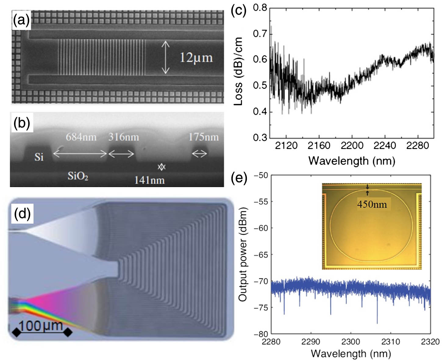
Silicon has been the material of choice of the photonics industry over the last decade due to its easy integration with silicon electronics, high index contrast, small footprint, and low cost, as well as its optical transparency in the near-infrared and parts of mid-infrared (MIR) wavelengths (from 1.1 to 8 μm). While considerations of micro- and nano-fabrication-induced device parameter deviations and a higher-than-desirable propagation loss still serve as a bottleneck in many on-chip data communication applications, applications as sensors do not require similar stringent controls. Photonic devices on chips are increasingly being demonstrated for chemical and biological sensing with performance metrics rivaling benchtop instruments and thus promising the potential of portable, handheld, and wearable monitoring of various chemical and biological analytes. In this paper, we review recent advances in MIR silicon photonics research. We discuss the pros and cons of various platforms, the fabrication procedures for building such platforms, and the benchmarks demonstrated so far, together with their applications. Novel device architectures and improved fabrication techniques have paved a viable way for realizing low-cost, high-density, multi-function integrated devices in the MIR. These advances are expected to benefit several application domains in the years to come, including communication networks, sensing, and nonlinear systems.
Integrated optics devices Waveguides Infrared Photonic integrated circuits Photonics Research
2018, 6(4): 04000254
1 Omega Optics Inc., Austin, TX, 78757, USA
2 Department of Electrical and Computer Engineering, University of Texas at Austin, Austin, TX, 78712, USA
3 School of Electronic Science and Engineering, Nanjing University, Nanjing 210093, China
In this paper, we reviewed the design principles of two-dimensional (2D) silicon photonic crystal microcavity (PCM) biosensors coupled to photonic crystal waveguides (PCWs). Microcavity radiation loss is controlled by engineered the cavity mode volume. Coupling loss into the waveguide is controlled by adjusting the position of the microcavity from the waveguide. We also investigated the dependence of analyte overlap integral (also called fill fraction) of the resonant mode as well as the effect of group index of the coupling waveguide at the resonant wavelength of the microcavity. In addition to the cavity properties, absorbance of the sensing medium or analyte together with the affinity constant of the probe and target biomarkers involved in the biochemical reaction also limits the minimum detection limits. We summarized our results in applications in cancer biomarker detection, heavy metal sensing and therapeutic drug monitoring.
photonic crystal (PC) sensor photonic crystal (PC) sensor biosensor biosensor slowlight slowlight photonic crystal microcavity (PCM) photonic crystal microcavity (PCM) photonic crystal waveguide (PCW) photonic crystal waveguide (PCW) high sensitivity high sensitivity high specificity high specificity photonic integrated circuits (PICs) photonic integrated circuits (PICs) nanophotonics nanophotonics Frontiers of Optoelectronics
2016, 9(2): 206


